Intel Foundry and ASML Expand High-NA EUV Deployment: Over 1 Million Wafers Processed as AI Chip Race Intensifies
Intel Foundry and ASML have deepened their strategic partnership around High-NA EUV lithography, confirming over one million wafers processed across R&D and production. As demand for massive multi-die AI accelerators surges, Intel's early adoption of 0.55 NA systems and anamorphic photomasks positions it ahead of TSMC in next-generation extreme density fabrication.

By Ajinkya Pawar
Head of Search & AI Intelligence • The AI NEWS
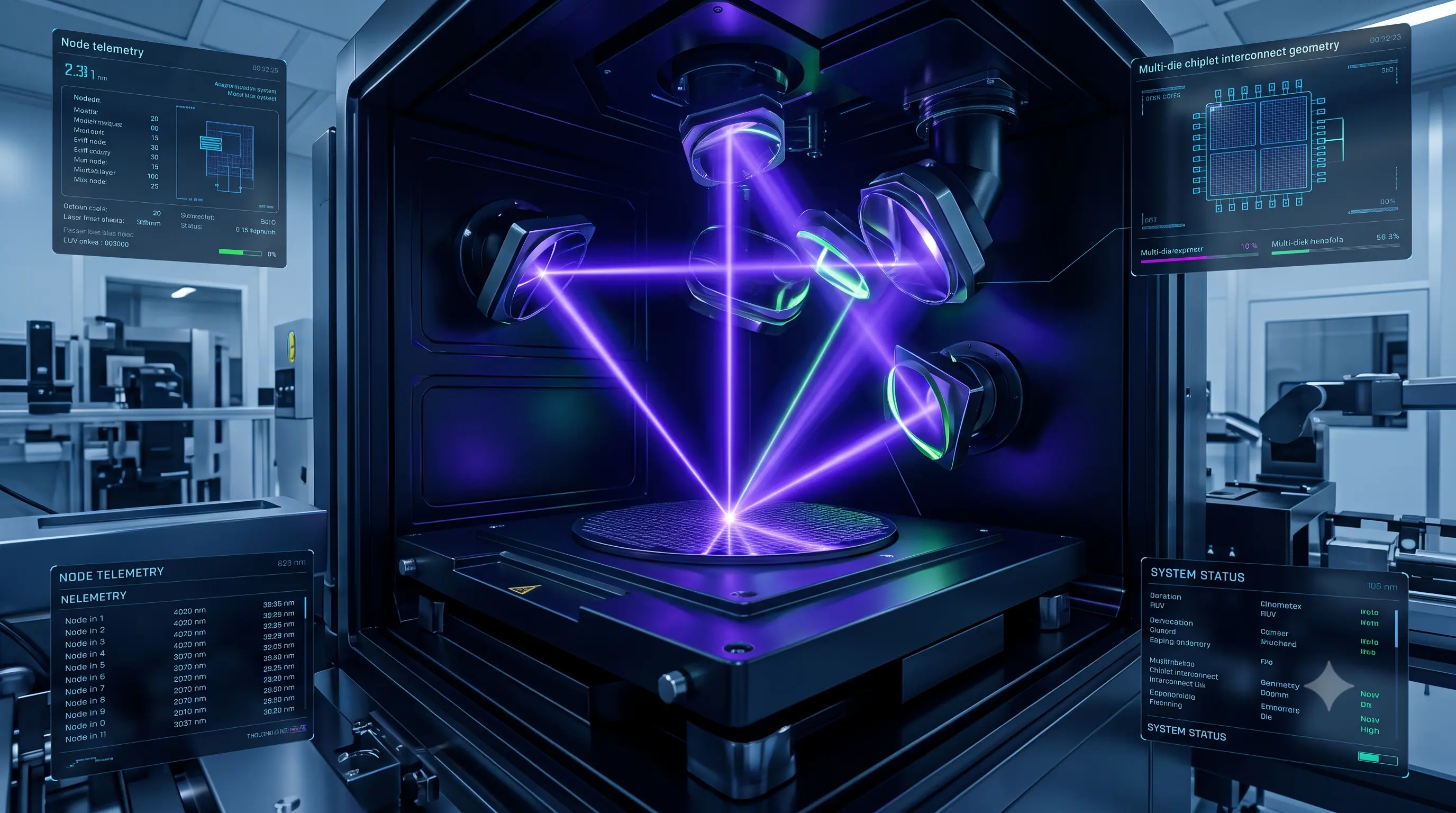
Key Developments & Executive Briefing
Fleet Utilization Record
Milestone1M+ WafersIntel has processed over one million High-NA EUV wafers across its Oregon Fab 25 facility, outpacing the rest of the semiconductor industry combined.
Transition from 18A to 14A
Architecture0.55 NASelected layers of Core Ultra Series 3 (Panther Lake) logic are dual-qualified on High-NA EUV, paving the way for full 14A node volume production by 2028.
Solving Anamorphic Half-Fields
Packaging6x12" MasksIntel and ASML are standardizing enlarged 6x12-inch reticles to eliminate reticle-stitching bottlenecks for gigantic multi-die AI accelerator packages.
At the SPIE Photomask Technology and Extreme Ultraviolet Lithography conference in Monterey, California, Intel Foundry and ASML officially announced an expanded strategic collaboration to accelerate the industrial deployment of High-NA EUV lithography. Intel confirmed that its fabrication facilities have now processed more than one million High-NA EUV wafers across research, tool certification, and commercial pilot runs—surpassing the cumulative output of the rest of the semiconductor industry combined.
The announcement comes as frontier AI model training and dense reasoning architectures push wafer fabrication to unprecedented physical limits. Modern gigawatt-scale datacenters demand larger, thermally dense multi-die chiplets with tens of billions of transistors etched into microscopic surface areas. While legacy low-numerical aperture EUV systems require multiple patterning exposures, mask alignments, and chemical etching cycles to achieve single-digit nanometer features, High-NA systems utilize an advanced 0.55 numerical aperture optical assembly to pattern critical layers in a single pass.
Independent Verification & The Foundry Lithography Split
A closer examination of the semiconductor manufacturing ecosystem reveals a stark strategic divergence between Intel Foundry and its chief rival, TSMC. Intel has positioned itself as the pioneer customer for ASML's next-generation hardware, currently operating two TWINSCAN EXE:5000 development tools and integrating the production-grade EXE:5200B scanner at its Hillsboro, Oregon campus. The newer EXE:5200B delivers throughput of approximately 175 wafers per hour with 0.7 nanometer overlay precision.
Intel has already qualified select critical layers of its Intel 18A process node—the foundation for the newly ramping Intel Core Ultra Series 3 "Panther Lake" processors—on High-NA systems. These layers are dual-qualified alongside existing Low-NA NXE scanners to maintain identical baseline defect density and manufacturing yield.
In contrast, TSMC has deliberately deferred commercial High-NA adoption until at least 2029. TSMC's leadership has calculated that the astronomical capital cost of High-NA tools—exceeding €350 million per scanner—makes aggressive multi-patterning on depreciated 0.33 NA scanners more economically viable for its high-volume N2 and A16 nodes. By accepting the early capital expense and steep engineering learning curve today, Intel aims to leapfrog TSMC in operational mastery ahead of its fully High-NA architected Intel 14A process node, slated for risk production in 2027 and volume manufacturing in 2028.
Overcoming the Anamorphic Half-Field Dilemma for AI Accelerators
Beyond raw resolution, the most critical dimension of the deepened Intel-ASML partnership addresses the physical constraints of AI accelerator design: reticle size. Because High-NA optics employ an anamorphic 8x demagnification in the scanning axis while maintaining 4x demagnification horizontally, the maximum reticle field size is halved to 26mm by 16.5mm.
For consumer mobile chips, a half-field reticle is easily accommodated. However, enterprise AI accelerators from NVIDIA, AMD, and hyperscaler custom silicon programs frequently push the reticle boundary to maximize silicon surface area. Designing monolithic dies or tightly coupled chiplet interposers across a split half-field requires complex "reticle stitching," which introduces severe overlay alignment tolerances, higher mask costs, and structural defect vulnerabilities.
To solve this architectural hurdle, Intel Foundry and ASML are co-developing standardized 6-inch by 12-inch oversized photomasks and advanced beam-shaping algorithms. By doubling the mask dimension, engineers can expose significantly larger continuous field areas without stitch lines, unlocking native fabrication of mega-die AI accelerators that would otherwise be cost-prohibitive or structurally unviable on competitive foundry lines.
Strategic Implications for AI Infrastructure Architects
For technology executives, cloud architects, and enterprise procurement directors, this milestone signals a critical structural shift in the global semiconductor landscape:
- 1.Supply Chain Redundancy for Frontier Accelerators: As hyperscalers seek to diversify their silicon sourcing away from total single-foundry dependence on TSMC, Intel Foundry's validated High-NA execution positions it as a viable destination for custom accelerator design starts on Intel 14A.
- 2.Defect Density & Cycle Time Reduction: By eliminating two to three mask exposures per critical metal layer, High-NA reduces fab cycle time by up to 20%, directly accelerating the turnaround time between silicon design tape-outs and packaged chip deliveries.
- 3.Packaging Integration: Lithography can no longer be viewed in isolation. As High-NA enables sub-10nm feature pitches on compute dies, advanced packaging interconnects (such as Intel EMIB and Foveros Direct) must advance concurrently to prevent packaging thermal resistance from bottlenecking compute density.
Intel's one-million-wafer milestone demonstrates that High-NA EUV has crossed the chasm from experimental laboratory hardware into repeatable industrial production. As chipmakers prepare for the trillion-parameter AI workload wave, the ability to pattern denser logic with fewer mask defects will define the next decade of compute dominance.
Fact-Checked Sources & Verified References
Sources & References
Related Coverage
Anthropic Projects Consecutive Quarterly Profitability as Enterprise Claude Demand Defies Foundation Model Margin Squeeze
AI & ModelsAnthropic Selects Nasdaq for Landmark Public Listing as Frontier AI Commercialization Accelerates
AI & ModelsAnthropic CEO Dario Amodei: 'For Too Long the Industry Lied' About Frontier AI Risks as Tech Leaders Back Slowdown Calls
Discussion (0)
Be the first to share insights on this story.